
Related Images

Download:
| Tiny | 192x128 | View | Download |
| Original svg | 300x200 | View | Download |
| Original as jpg | 300x200 | View | Download |
This image was acquired from
wikimedia. It was marked as Public Domain or CC0 and is free to use. To verify, go to the source and check the information there.
Looking for more info about this image?
Try a Google Reverse Image Search for it.
Try a Google Reverse Image Search for it.
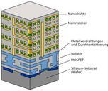
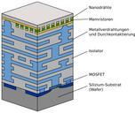
Keywords from Image Description:
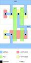
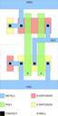
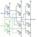
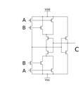
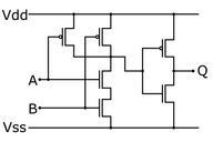
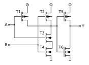
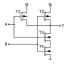
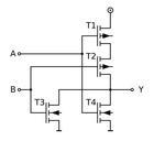
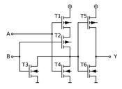
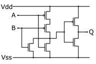
CMOS OR.svg ValidSVG made with Inkscape Layout of NMOS and PMOS components in an OR Gate This OR gate is implemented as an AND gate with both inputs inverted by using PMOS at the top as well as the otutput inverter at the right which is functionally correct but is not commonly used as it requires extra transistors Own drawing Inkscape