
Related Images


Download:
| Tiny | 227x128 | View | Download |
| Original svg | 400x225 | View | Download |
| Original as jpg | 400x225 | View | Download |
This image was acquired from
wikimedia. It was marked as Public Domain or CC0 and is free to use. To verify, go to the source and check the information there.
Looking for more info about this image?
Try a Google Reverse Image Search for it.
Try a Google Reverse Image Search for it.
Keywords from Image Description:
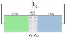
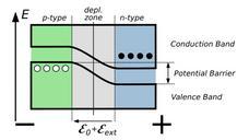
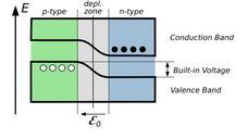
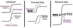
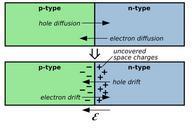
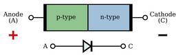
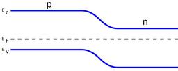
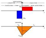
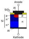
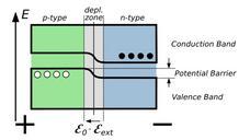
ForwardBiased pn Junction Bands.svg Diagram of pn junction under forward bias showing conduction and valence bands the depletion zone the potential barrier the resultant electric field mathcal mathcal ext and the types of semiconductor Own drawing done in Inkscape inductiveload UnBiased pn Junction Reverse Biased pn Junction PNjunction