Download:
| Tiny | 284x128 | View | Download |
| Small | 569x256 | View | Download |
| Original png | 957x430 | View | Download |
| Original as jpg | 957x430 | View | Download |
This image was acquired from
wikimedia. It was marked as Public Domain or CC0 and is free to use. To verify, go to the source and check the information there.
Looking for more info about this image?
Try a Google Reverse Image Search for it.
Try a Google Reverse Image Search for it.
Keywords from Image Description:
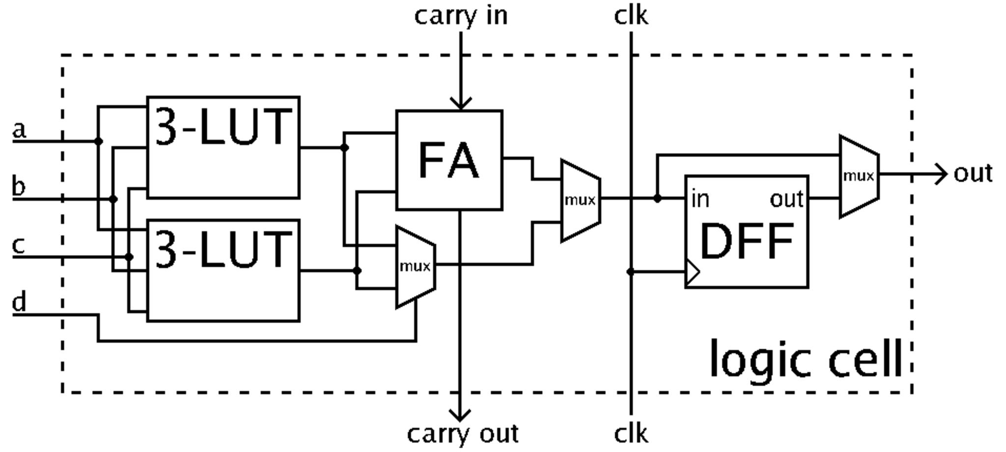
FPGA cell example. en An example of how an FPGA logic cell can look like incl inp LUT or two LUTs Full Adder and Dtype Flip Flop The muxes to the right have their select signal set during the programming of the cell sv Exempel hur en logisk cell en FPGA kan vara uppbyggd inkl en LUT eller tv LUTar en Fulladderare och en Dflipflop
