
Related Images


Download:
| Tiny | 240x128 | View | Download |
| Small | 480x256 | View | Download |
| Medium | 960x512 | View | Download |
| Large | 1920x1024 | View | Download |
| Original png | 3000x1600 | View | Download |
| Original as jpg | 3000x1600 | View | Download |
This image was acquired from
wikimedia. It was marked as Public Domain or CC0 and is free to use. To verify, go to the source and check the information there.
Looking for more info about this image?
Try a Google Reverse Image Search for it.
Try a Google Reverse Image Search for it.
Keywords from Image Description:
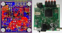
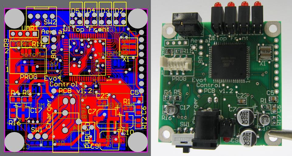
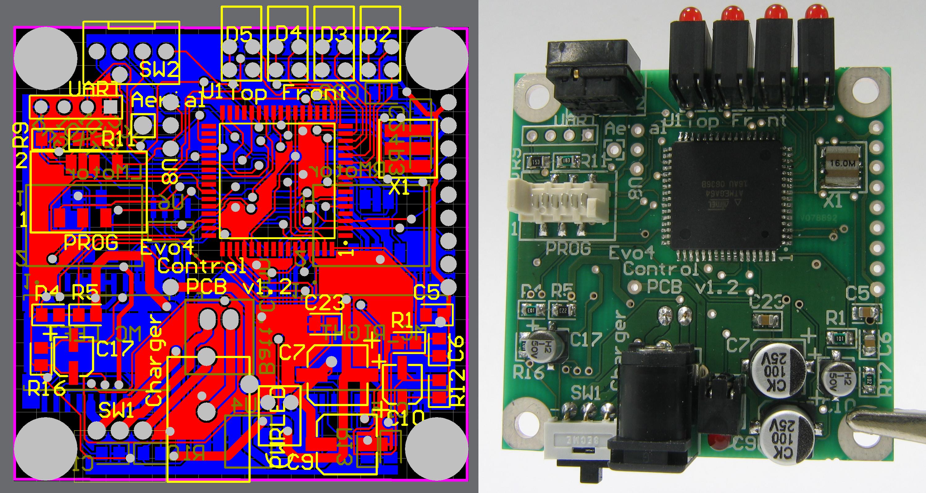
PCB design and realisation smt and through hole. printed circuit board PCB layout created on computer and right the manufactured board populated with parts Both throughhole and surface mounts components have been used the board is doublesided with throughhole plating green solder resist white solder paste visible on unsoldered holes