
Related Images


Download:
| Tiny | 72x128 | View | Download |
| Small | 145x256 | View | Download |
| Medium | 290x512 | View | Download |
| Large | 581x1024 | View | Download |
| Original | 1336x2352 | View | Download |
This image was acquired from
wikimedia. It was marked as Public Domain or CC0 and is free to use. To verify, go to the source and check the information there.
Looking for more info about this image?
Try a Google Reverse Image Search for it.
Try a Google Reverse Image Search for it.
Keywords from Image Description:
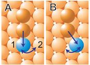
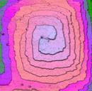
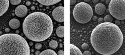
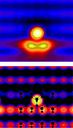
Scanning tunneling microscope Semiconductor Spintronics . Left high resolution STM image of manganese atom the red area between the larger blob and the two smaller blobs which are arsenic atoms that has been substituted for indium atom larger blob on the indium arsenide substrate Right The theoretical model of the configuration the