
Related Images


Download:
| Tiny | 129x128 | View | Download |
| Small | 258x256 | View | Download |
| Medium | 517x512 | View | Download |
| Original | 909x900 | View | Download |
This image was acquired from
wikimedia. It was marked as Public Domain or CC0 and is free to use. To verify, go to the source and check the information there.
Looking for more info about this image?
Try a Google Reverse Image Search for it.
Try a Google Reverse Image Search for it.
Keywords from Image Description:
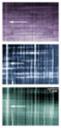
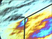
Silicon Wafer . new NIST calibration system under development used infrared laser light to precisely measure the thickness of millimeter silicon wafers Changes in color within the spatial map above represent changes in wafer thickness Green represents the average wafer thickness while red orange and yellow areas are thicker and