Related Images


This image was acquired from
wikimedia. It was marked as Public Domain or CC0 and is free to use. To verify, go to the source and check the information there.
Looking for more info about this image?
Try a Google Reverse Image Search for it.
Try a Google Reverse Image Search for it.
Keywords from Image Description:
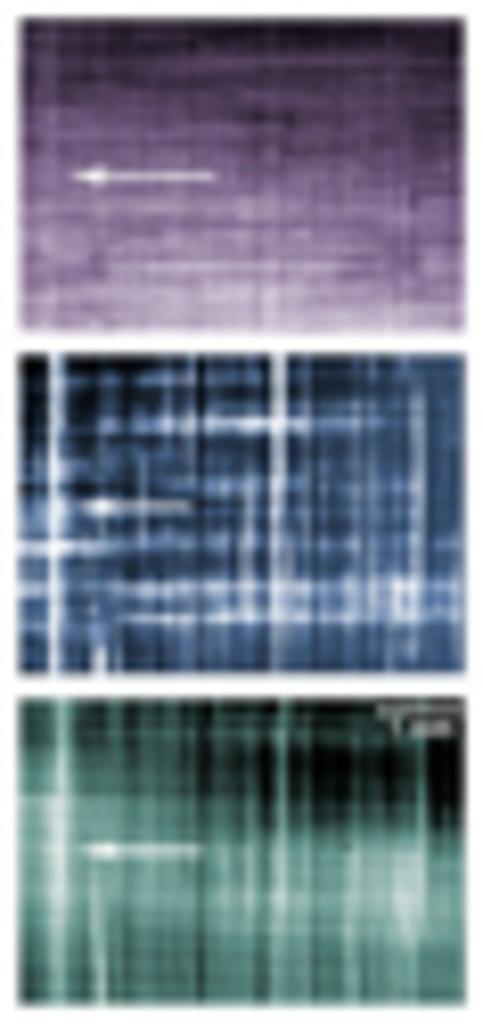
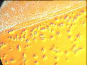
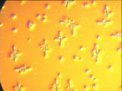
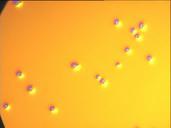
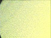
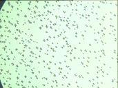
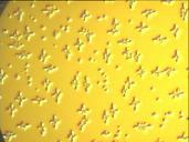
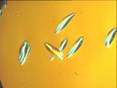
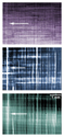
Strained Silicon Devices . Xray topographs of three different strata of strainedsilicon wafer show close correspondence in defects from the base silicon layer top through the final strainedsilicon layer bottom Color has been added for contrast one particular defect area is highlighted Courtesy National Institute of Standards and