
Related Images


Download:
| Tiny | 130x128 | View | Download |
| Original png | 190x186 | View | Download |
| Original as jpg | 190x186 | View | Download |
This image was acquired from
wikimedia. It was marked as Public Domain or CC0 and is free to use. To verify, go to the source and check the information there.
Looking for more info about this image?
Try a Google Reverse Image Search for it.
Try a Google Reverse Image Search for it.
Keywords from Image Description:
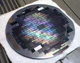
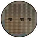
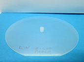
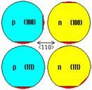
Wafer flats convention. Wafer flats conventionv svg file to replace JPEG of same name Conventional meaning of flats in semiconductor wafers Red denotes material that has been removed Wafers under mm generally have flats indicating crystallographic planes of high symmetry usually the face and in oldfashined wafers those below about