
Related Images


Download:
| Tiny | 137x128 | View | Download |
| Small | 274x256 | View | Download |
| Medium | 549x512 | View | Download |
| Large | 1099x1024 | View | Download |
| Original | 1800x1677 | View | Download |
This image was acquired from
wikimedia. It was marked as Public Domain or CC0 and is free to use. To verify, go to the source and check the information there.
Looking for more info about this image?
Try a Google Reverse Image Search for it.
Try a Google Reverse Image Search for it.
Keywords from Image Description:
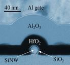
TEM of silicon nanowire . In this transmission electron micrograph silicon nanowire is shown surrounded by stack of thin layers of material called dielectrics which store electrical charge NIST scientists determined the best arrangement for this dielectric stack for the optimal construction of silicon nanowirebased memory devices